Understanding PCB Manufacturing: From Design to Production
Printed Circuit Boards (PCBs) form the structural and electrical foundation of modern electronic devices. From smart home systems to industrial control units, high-quality PCB manufacturing ensures stable circuit performance and long-term reliability.
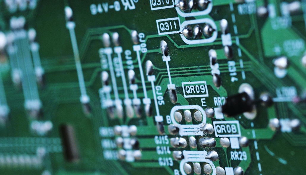
What Is a PCB?
A Printed Circuit Board (PCB) is a flat board made of insulating material with conductive copper traces that connect electronic components. The PCB provides mechanical support and electrical pathways for electronic circuits.
Key PCB Manufacturing Steps
1. PCB Design & Layout
The process begins with schematic design and PCB layout using CAD software. Engineers define trace width, component placement, and signal routing to ensure electrical performance and heat management.
2. Material Selection
Common materials include FR-4, aluminum substrate, and high-frequency laminates. Material selection impacts durability, signal integrity, and thermal performance.
3. Copper Pattern Etching
Copper layers are etched to create conductive pathways. Precision at this stage determines electrical stability.
4. Drilling & Plating
Via holes are drilled and plated to create inter-layer electrical connections in multilayer PCBs.
5. Solder Mask & Silkscreen
A solder mask protects copper traces from oxidation and short circuits. Silkscreen markings identify components and circuit areas.
Why PCB Quality Matters
High-quality PCB manufacturing ensures:
Signal integrity
Thermal stability
Long service life
Reduced failure rate
Compliance with IPC standards
Modern electronics demand precision-engineered PCBs capable of handling high-density and high-speed circuits.